
VNA frequency-domain measurement
A vector network analyzer (VNA) tests a device at selected frequencies and measures both the magnitude and phase of its reflected and transmitted signals. The result is a complex S-parameter at each frequency. The VNA time-domain reflection note uses frequency measurements to calculate a synthetic impulse response; this note stays in the frequency domain and follows the VNA inductor S-parameters REPL example. Keysight's frequency-domain overview describes direct VNA sweeps of a device under test.
What the test receivers measure
For a two-port device driven at port 1, let
The first index names the responding port; the second names the driven port. These are complex ratios, so a dB plot shows only their magnitudes. The phase remains available in the complex readings. See S-parameters for the novice for the wave definitions and an inductor calculation. Rohde & Schwarz's S-parameter primer also explains reflection, transmission, magnitude, and phase.
Choose frequencies directly
The inductor example analyzes a 5 nH series inductor from 1 to 3 GHz:
var g = nP.global;
g.fList = g.fGen(1e9, 3e9, 101);

var tx = nP.mod({
  mode: 'VNA-frequency',
  fList: g.fList
});
fGen() includes both endpoints. The 101 values give 100 intervals, each 20 MHz wide. VNA-frequency accepts any nonempty, strictly increasing list of nonnegative frequencies; equal spacing is not required. mod() puts a unit complex reference at each listed frequency and makes the circuit's fList match. The points represent independent tones in a sweep, not FFT bins of a sampled waveform. There is no tList, sample rate, Nyquist limit, or inverse FFT in this mode. A physical VNA applies frequencies in sequence; nP calculates their independent steady-state responses.
Connect the ideal measurement paths
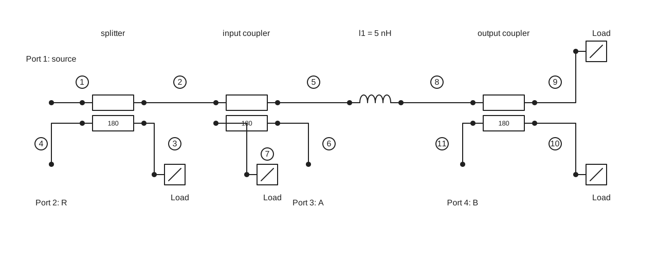
The REPL circuit first uses a default Coupler180() as a matched equal splitter. Its port 4 feeds reference receiver R, while port 2 drives the input coupler. The input coupler's port 2 drives the inductor and port 3 feeds reflection receiver A. The output coupler's port 4 feeds transmission receiver B. Unused ports are matched.
source -> splitter -> input coupler -> 5 nH inductor -> output coupler
              |            |                                   |
              R            A                                   B
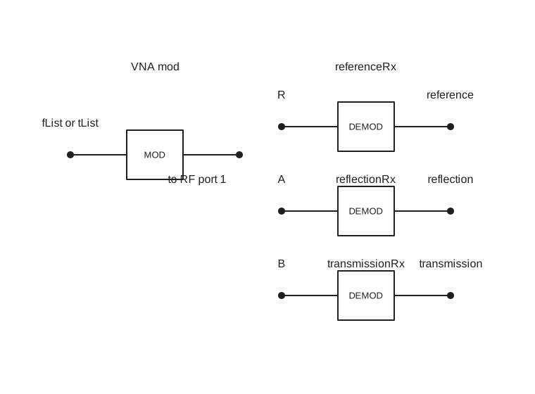
The nP.nodal() result exposes four ports: source input, R, A, and B. Its three demodulators select external output ports 2, 3, and 4. Every unused coupler port is matched.
Compare all three receivers
Each default coupler has an equal-power split. Its through-wave voltage factor
For the unit source used by mod(), the raw complex receiver voltages are:
The receiver settings are R gain 1, A gain 2, and B gain 2. A and B each specify referenceReceiver: referenceRx, so the receiver divides by R's complex phasor before applying its settable gain. Thus 2A/R=S_{11} and 2B/R=S_{21}. The gain defaults to 1, including for a direct mod-to-demod connection. nP does not infer these settings from the VNA mode or inspect arbitrary fixture paths.
There is no attenuator in any of the three VNA REPL circuits. The three ideal couplers split power without dissipating it. A 3 dB pad in front of R would be a different fixture: it would lower R's raw voltage by VNA-frequency and VNA-time do not assign gains on their own.
var referenceRx = nP.demod(circuit, {
  outputPort: 2,
  referenceGain: 1,
  noise: false
});
var reflectionRx = nP.demod(circuit, {
  outputPort: 3,
  referenceReceiver: referenceRx,
  referenceGain: 2,
  noise: false
});
var transmissionRx = nP.demod(circuit, {
  outputPort: 4,
  referenceReceiver: referenceRx,
  referenceGain: 2,
  noise: false
});

var s11Table = reflectionRx.out('response dB');
var s21Table = transmissionRx.out('response dB');

nP.lineChart({inputTable: [s11Table], title: 'Measured S11', metricPrefix: 'giga'});
nP.lineChart({inputTable: [s21Table], title: 'Measured S21', metricPrefix: 'giga'});
For the complete circuit construction, run VNA inductor S-parameters. The receiver also offers out('response magnitude'), out('response phase') in degrees, out('response real'), and out('response imaginary') as numeric tables. Its out('spectrum') retains the raw receiver phasors, and out('frequencies') returns the swept hertz values.
Check one point at 2 GHz
The series inductor's impedance is
The receiver values and the direct nP.L(5e-9) S-parameters agree:
| Quantity at 2 GHz | Reflection path | Transmission path |
|---|---|---|
| Raw receiver voltage | ||
| After dividing by R and applying gain 2 | ||
| Corresponding inductor parameter | ||
| Magnitude | 0.532018 | 0.846733 |
| Magnitude in dB | −5.481473 dB | −1.445070 dB |
| Phase | +57.858° | −32.142° |
The raw complex values retain the signs of their imaginary parts. Division by R removes the source/splitter level; the factor of two removes the coupler sampling factor. The direct inductor table comes from l1.out('s11dB', 's21dB'); it provides an independent check of the two test paths.
Relationship to the time-domain mode
| Question | VNA-frequency | VNA-time |
|---|---|---|
| Starting grid | Supplied fList | Power-of-two tList starting at zero |
| Frequencies | Selected directly; may be uneven | Generated DC-to-Nyquist FFT grid |
| Receiver result | Complex tone response at each frequency | Synthetic time-domain waveform |
| Inverse FFT | None | Used by demod().out('waveform') |
| Example | Three receivers measuring a 5 nH inductor | Same receiver fixture with a 5 nH inductor, or R/A locating cable faults |
The VNA inductor impulse response example uses this same three-receiver circuit with VNA-time. Its 4,096-point tList generates an equally spaced DC-to-8 GHz grid; A and B are divided by R and corrected by the same settable gain of 2 before the inverse FFT. Their plotted outputs are the normalized reflection and transmission impulse responses. The time-domain reflection note explains that grid and the three plots.
Here the direct 1-to-3 GHz sweep reports frequency-domain S-parameters. Its 20 MHz point spacing does not create a time record or a displayed travel time. The ideal couplers have no finite bandwidth or mismatch. VNA-frequency supports deterministic demod() reception with noise: false; it does not simulate receiver noise.