Symbol library
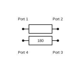
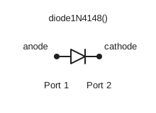
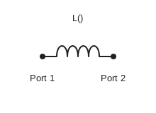
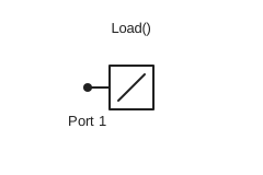
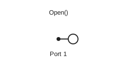
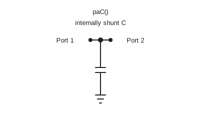
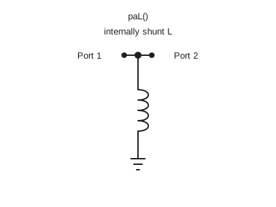
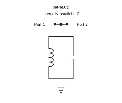
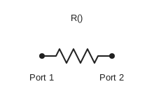
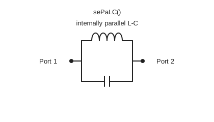
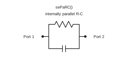
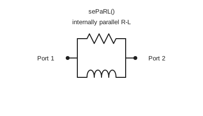
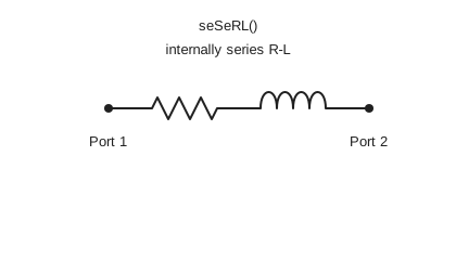
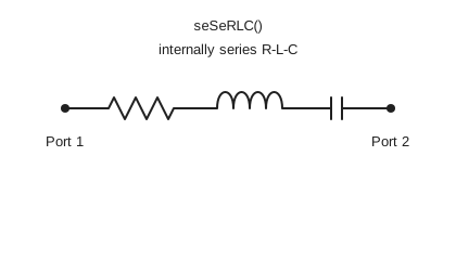
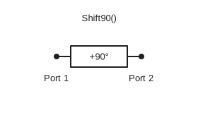
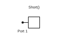
These are the canonical SVG symbols used by nP schematics. Each drawing shows its terminal or connector numbering. Names above a drawing identify the constructors or drawing names that share it. Select a symbol to open the original SVG at full size.
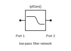
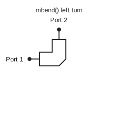
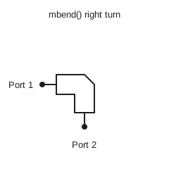
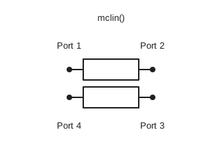
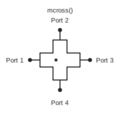
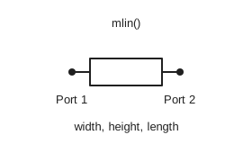
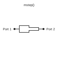
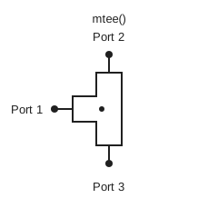
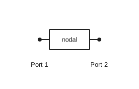
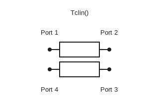
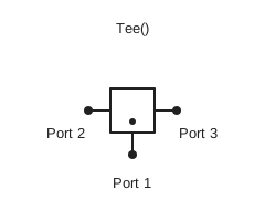
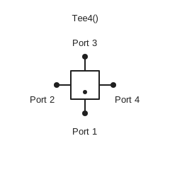
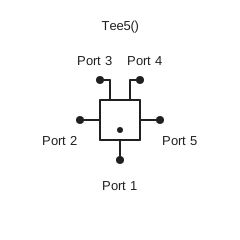
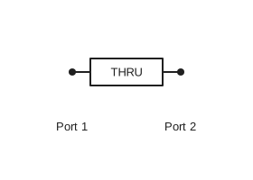
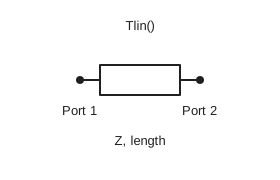
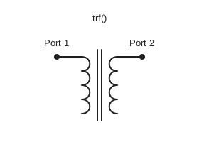
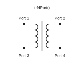
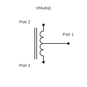
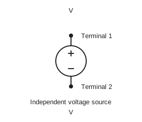
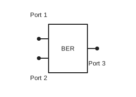
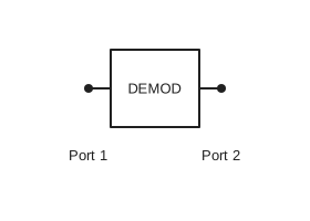
RF terminal numbers follow the constructor's public port order. Signal-block connectors describe signal flow and are not RF ports. Source and device artwork listed separately has no numerical constructor; selecting that artwork does not create an electrical model.
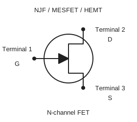
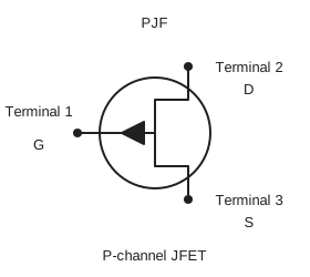
NJF and PJF are implemented JFET constructors and drawing names, with terminals 1 gate, 2 drain, 3 source. These numbers describe the drawing, not a physical package pinout. They work in schematic descriptions without a frequency grid:
var description = {
    paths: ['1 right J1=NJF[1,2,3] 1 2 3']
};

var drawing = nP.schematic(description);
Use PJF for the P-channel symbol. nP.NJF() and nP.PJF() provide level-1 DC, RF, approximate noise and weak nonlinear analysis. See JFET models. Schematic descriptions select artwork without executing a numerical constructor.
MESFET and the drawing-only HEMT share the N-channel FET artwork and the same gate/drain/source terminal order. For example, '1 right Q1=HEMT(HEMT)[1,2,3] 1 2 3' labels a HEMT drawing. nP.MESFET() supplies a Statz/MES1 SPICE reference profile, not a commercial fit. HEMT has no numerical constructor. Shared geometry does not select device material or a numerical model.
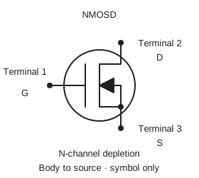
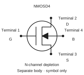
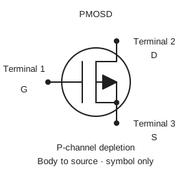
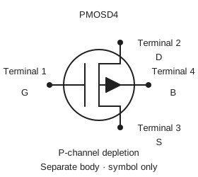
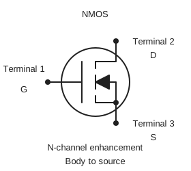
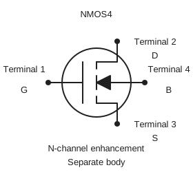
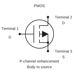
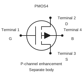
MOSFET artwork uses the same 1 gate, 2 drain, 3 source order. Four-terminal drawings add 4 body:
| Drawing names | Mode | Body connection |
|---|---|---|
NMOS, PMOS | Enhancement; broken channel | Internally tied to source |
NMOS4, PMOS4 | Enhancement; broken channel | Separate terminal 4 |
NMOSD, PMOSD | Depletion; continuous channel | Internally tied to source |
NMOSD4, PMOSD4 | Depletion; continuous channel | Separate terminal 4 |
For example, '1 right M1=NMOS4[1,2,3,4] 1 2 3 4' preserves the independent body connection. Use the three-terminal artwork only when the body is tied to source. nP.NMOS() and nP.PMOS() now provide numerical enhancement models. Set body: 'external' for their four-terminal forms; NMOS4/PMOS4 remain drawing aliases, not constructor names. Depletion names remain artwork only. See MOSFET models.
The current description layout rejects direct self-connections made by assigning the same node to two terminals on one component. Use the three-terminal symbol for an internal body/source tie; other requested self-connections remain a layout limitation.
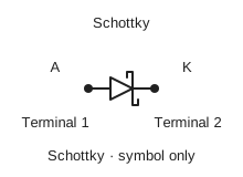
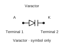
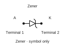
Specialized diode artwork uses 1 anode, 2 cathode:
| Drawing name | Distinguishing mark |
|---|---|
Schottky | Hooked cathode bar |
Zener | Angled cathode-bar ends |
Varactor | Two parallel cathode plates |
A description path such as '1 right D1=Varactor 2' draws the symbol. These names have no numerical constructors and do not supply DC, RF, noise or intermodulation behavior. Existing D() and diode1N4148() models retain their ordinary diode artwork and behavior.
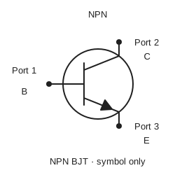
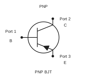
HBT and PIN drawings reuse existing geometry with an instance caption: '1 right Q1=NPN(HBT)[1,2,3] 1 2 3' (or PNP) and '1 right D1=D(PIN) 2'. HBT terminal order remains base, collector, emitter. These description captions do not select an HBT or PIN numerical model.
See Schematics for drawing circuits and RF constructors for numerical component behavior.
81 canonical symbols. The gallery uses the original artwork and catalog directly.
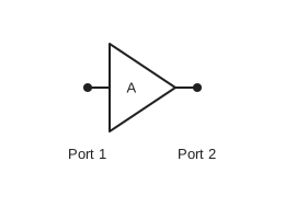
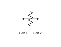
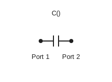
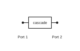
RF components and networks
Signal and analysis blocks
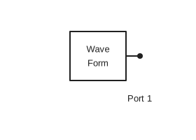
Source artwork
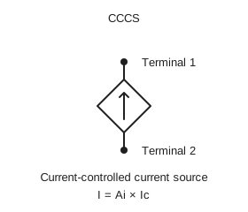
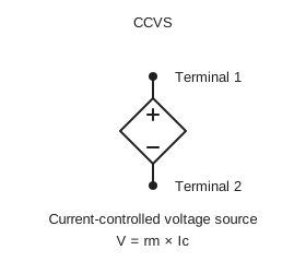
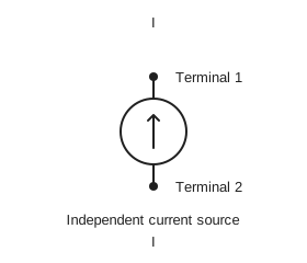
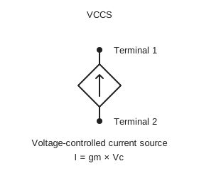
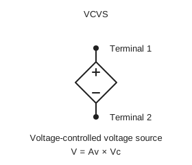
Device artwork