
Transistors and Diodes
The public active-device constructors are nP.Amp(), nP.D(), nP.diode1N4148(), nP.NPN(), nP.PNP(), nP.NJF(), nP.PJF(), nP.NMOS() and nP.PMOS(). The amplifier is a configurable two-port gain/noise model. Diode and transistor models combine DC I–V curves with RF behavior at a fixed bias.
NPN transistor
nP.NPN() supports 2N3904 (default) and BFR93A. It returns a three-port: 1 base, 2 collector, 3 emitter.
// NPN curve tracer and RF at a selected Q point
var g = nP.global;
g.fList = g.fGen(10e6, 500e6, 51);

var q1 = nP.NPN({
    model: '2N3904',
    configuration: 'commonEmitter',
    bias: {
        ib: {start: 0, stop: 50e-6, points: 6},
        vce: {start: 0, stop: 10, points: 201}
    },
    qPoint: {ib: 20e-6, vce: 5},
    temperature: g.Temp
});
var short = nP.Short();
var amplifier = nP.nodal(
    [q1, 1, 2, 3],
    [short, 3],
    ['out', 1, 2]
);
var curves = q1.ivTable();
var rf = amplifier.out('s11dB', 's21dB');
var stability = amplifier.out('K', 'deltaMag');
var noise = amplifier.out('NF21dB');

nP.lineChart({inputTable: [curves], metricPrefix: 'none',
    title: '2N3904 curve tracer', xAxisTitle: 'VCE (V)', yAxisTitle: 'IC (A)'});
nP.lineChart({inputTable: [rf], metricPrefix: 'mega', title: 'Common-emitter RF'});
bias defines the curves; qPoint fixes the RF operating point. Sweeping does not move it. Construct another NPN with different qPoint values to select another point. With no arguments, the constructor uses the defaults above and the current global.fList, initially [2e9], just as R() does. Partial nested settings keep omitted defaults.
For commonBase, use bias: {ie: {...}, vcb: {...}} and qPoint: {ie: 2e-3, vcb: 5}; its table plots IC versus VCB at stepped outward IE. For commonCollector, retain IB and positive VCE; the table reports outward IE. The DC configuration does not terminate an RF port: ground emitter, base or collector externally to obtain the corresponding RF configuration. .bias, .qPoint, .smallSignal and .model expose the chosen point, linearization and provenance.
Completed two-ports provide .stability and .out('K', 'deltaMag'). Unconditional small-signal stability requires K > 1 and |Δ| < 1. K comes from the final S-parameters; intermediate K < 1 is allowed. Bare three-port NPNs have no two-port K value.
BFR93A includes its published SOT23 L/C network. The 2N3904 card includes terminal resistances but no explicit package L/C model. Noise uses classical shot/thermal sources, without fitted excess-noise or high-frequency induced-noise behavior. With global.twoTone set before construction, IM/OIP selectors use direct Taylor current and charge terms; they omit quadratic remixing, compression and harmonic balance. Neither card models avalanche or self-heating. External DC bias-network solving remains future work.
Try NPN curve tracer and RF in the REPL.
PNP transistor
nP.PNP() supports 2N3906 using the same model engine and APIs as NPN. Its ports remain 1 base, 2 collector, 3 emitter. Use physical signed PNP values:
// PNP curve tracer and RF
var g = nP.global;
g.fList = g.fGen(10e6, 500e6, 51);
var q1 = nP.PNP({
    model: '2N3906',
    configuration: 'commonEmitter',
    bias: {
        ib: {start: 0, stop: -50e-6, points: 6},
        vce: {start: 0, stop: -10, points: 201}
    },
    qPoint: {ib: -20e-6, vce: -5},
    temperature: g.Temp
});
var short = nP.Short();
var amplifier = nP.nodal(
    [q1, 1, 2, 3],
    [short, 3],
    ['out', 1, 2]
);
var curves = q1.ivTable();
var rf = amplifier.out('s11dB', 's21dB');
nP.lineChart({inputTable: [curves], metricPrefix: 'none',
    title: '2N3906 curve tracer', xAxisTitle: 'VCE (V)', yAxisTitle: 'IC (A)'});
nP.lineChart({inputTable: [rf], metricPrefix: 'mega', title: 'PNP common-emitter RF'});
nP.schematic(amplifier);
PNP() with no options uses these defaults and the current frequency context. IB and IC are negative. The reported outward IE is negative too: current physically enters the emitter. Curves retain their 0-to-negative sweep order; they do not change the RF Q point. For common base use negative ie/vcb, defaulting to qPoint: {ie: -2e-3, vcb: -5}. Common collector uses negative IB/VCE and plots outward IE. Configuration selects DC constraints; the RF network still needs explicit terminal connections.
PNP supplies its own active noise covariance and bias-dependent nonlinear coefficients, and its completed two-port supports K. The 2N3906 card includes RB/RC but no explicit package L/C network. The NPN model limits and direct Taylor intercept approximation also apply here. The symbol's emitter arrow points inward; its numbered ports stay fixed during rotation or mirroring.
Try PNP curve tracer and RF in the REPL.
Amplifier
nP.Amp() defaults to a matched, unilateral 20 dB gain stage with 4 dB noise figure, referenced to 290 K. Its default S-parameters are frequency-flat across the selected list. The first two positional arguments change gain and noise figure; an options object supports measured S-parameters and other noise properties.
nP.global.fList = nP.global.fGen(1e9, 2e9, 11);

var amp1 = nP.Amp();      // 20 dB gain, 4 dB NF
var amp2 = nP.Amp(15, 3); // 15 dB gain, 3 dB NF

var gainAndNoise = amp2.out('s21dB', 'NF21dB');
nP.lineTable({inputTable: [gainAndNoise], title: 'Amplifier'});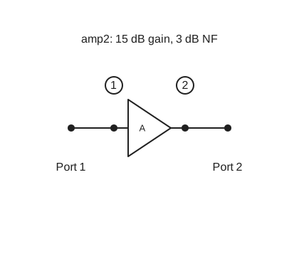
For two-tone intermodulation, the object form can supply oip2dBm, oip3dBm, and harmonicOip2dBm. None is present by default:
var amp3 = nP.Amp({
    gainDb: 20,
    noiseFigureDb: 4,
    oip3dBm: 30
});
The full options include spars, fMinDb, gammaOpt, noiseResistanceOhms, and referenceTemperature. See Noise and Intermodulation for measurement setup and the limits of the intercept calculation.
SPICE-style diode
nP.D() currently selects 1N4148, a silicon signal diode. Like the transistor constructors, it keeps the displayed DC sweep separate from an explicit RF Q point. Port 1 is the anode; port 2 is the cathode.
// 1N4148 curves and RF at a fixed operating point
var g = nP.global;
g.fList = g.fGen(10e6, 1e9, 51);

var d1 = nP.D({
    model: '1N4148',
    bias: {
        vd: {start: 0, stop: 0.8, points: 201}
    },
    qPoint: {vd: 0.6},
    temperature: g.Temp
});

var curves = d1.ivTable();
var response = d1.out('s11dB', 's21dB');
var noise = d1.out('NF21dB');
var fixedBias = d1.bias;

nP.log(fixedBias);
nP.schematic(d1);
nP.lineChart({
    inputTable: [curves],
    title: '1N4148 DC curve',
    xAxisTitle: 'Anode-to-cathode voltage (V)',
    yAxisTitle: 'Anode current (A)',
    metricPrefix: 'none'
});
nP.lineChart({
    inputTable: [response],
    title: '1N4148 RF at VD = 0.6 V',
    xAxisTitle: 'Frequency (MHz)',
    yAxisTitle: 'S-parameters (dB)',
    metricPrefix: 'mega'
});
These are also the defaults for D(), except that its frequency grid follows the current global.fList, initially [2e9]. Temperature follows global.Temp, initially 293 K. Partial nested options keep omitted defaults. vd means anode minus cathode, in volts; id is positive from anode to cathode, in amperes.
ivTable() returns a directly plottable table. ivTable({vd: {start: -5, stop: 0.8, points: 301}}) selects another curve range without moving the Q point. .bias and .qPoint report the solved currents and voltages; .smallSignal reports the bias-dependent conductance, resistance and capacitance. .model records the selected card and its provenance. .dc.bias records the sweep. Without a DC supply, RF networks preserve the device's selected bias. A supported nodal/cascade network containing V() automatically solves its external bias before rebuilding diode RF, noise and weak nonlinear data. Read network.operatingPoint; the original diode object and I–V curve settings stay unchanged.
The archived NXP SPICE card includes series resistance, leakage, junction charge and transit-time charge. It is a different parameter set from diode1N4148() below. It has no explicit package L/C network or large-signal transient simulation. Its noise follows classical SPICE junction shot noise plus resistor thermal noise; it does not model calibrated avalanche or excess noise. Weak nonlinear products use local current/charge derivatives and the existing two-tone analysis, with the same direct-source approximation described in Intermodulation.
Try 1N4148 DC and RF in the REPL. Other diode families and part numbers are not implemented in D() yet.
Legacy 1N4148 diode: RF and DC
nP.diode1N4148() returns a two-port series diode. Its default applied bias is 0 V, and its temperature defaults to nP.global.Temp. A new global context uses 293 K. The RF response is the small-signal behavior around the selected bias; the I–V method uses the same device parameters.
nP.global.fList = nP.global.fGen(100e6, 2.1e9, 101);

var diode = nP.diode1N4148({biasVoltage: 0});
var rfResponse = diode.out('s11dB', 's21dB');
var dcCurve = diode.ivTable(0, 0.8, 101);

nP.lineChart({
    inputTable: [rfResponse],
    title: '1N4148 RF response',
    metricPrefix: 'giga'
});
nP.lineChart({
    inputTable: dcCurve,
    title: '1N4148 forward I–V',
    metricPrefix: 'none',
    xAxisTitle: 'Voltage (V)',
    yAxisTitle: 'Current (A)'
});
ivTable(start, stop, points) returns a table headed ['vD', 'iD'], with volts and amperes. If you omit those arguments, the sweep defaults to −110 V through 1 V, 401 points. The default RF frequency list is the selected nP.global.fList; fList in the constructor options can override it.
Legacy diode options and defaults
| Option | Default | Meaning |
|---|---|---|
is | 2.75e-11 A | Saturation current. |
n | 2 | Ideality factor. |
rs | 0.568 Ω | Series resistance. |
cj0 | 4e-12 F | Zero-bias junction capacitance. |
vj | 0.75 V | Junction potential. |
m | 0.5 | Capacitance exponent. |
tt | 4e-9 s | Transit time. |
leakageResistance | 4e9 Ω | Parallel leakage resistance. |
breakdownVoltage | 100 V | Reverse-breakdown magnitude. |
biasVoltage | 0 V | Applied DC bias. |
temperatureK | nP.global.Temp | Device temperature. |
The model also accepts breakdownCurrent (default 100 µA), breakdownSoftness (default 2 V), and ivStart, ivStop, ivPoints for the default displayed I–V sweep.
Inspect the legacy bias point
The returned .diode metadata includes normalized parameters and the calculated bias point. This helps tie the RF response to the DC condition:
var diode = nP.diode1N4148({biasVoltage: 0.5});
var biasCurrent = diode.diode.bias.current;
var dynamicResistance = diode.diode.bias.dynamicResistance;
var totalCapacitance = diode.diode.bias.totalCapacitance;

nP.log(biasCurrent);       // amperes
nP.log(dynamicResistance); // ohms
nP.log(totalCapacitance);  // farads
The diode also supplies noise covariance and weak-signal IM2, IM3, and second-harmonic sources when used in the corresponding analyses. Its RF model is linearized at one bias point; it does not simulate large-signal switching, compression, or transient charge storage. See Noise and Intermodulation.
JFET transistors
NJF() and PJF() return 1 gate, 2 drain, 3 source. Defaults select onsemi MMBF5457LT1 and MMBFJ175LT1 silicon records. The shared SPICE level-1 model includes contact resistance, gate leakage and nonlinear junction charge.
nP.global.fList = nP.global.fGen(1e6, 100e6, 51);
var q1 = nP.NJF({qPoint: {vgs: -1, vds: 10}});
var curves = q1.ivTable({vgs: {points: 3}, vds: {points: 21}});
nP.lineChart({inputTable: [curves], title: 'JFET drain curves', metricPrefix: 'none'});
The NJF Q point above is the default; PJF defaults to VGS=+1 V and VDS=−10 V. Options are model, qPoint, bias, temperature (K), fList (Hz). Curves return VDS in volts and signed drain current in amperes, without changing RF bias. All three JFET currents enter the device. Networks with V() solve external bias first, then rebuild RF, noise and weak nonlinear data per placement. Without a supply, the constructor Q point remains the RF bias.
The commonSource schematic board covers self-bias with a gate resistor, drain load, AC coupling, optional source bypass and optional supply bypass, for either polarity. NLEV=1 channel/flicker noise has an ohmic-region limitation; gate shot/induced noise and measured package/noise fitting are absent. Direct Taylor intermodulation omits quadratic remixing and large-signal effects. MESFET now has a Statz reference profile; HEMT and advanced MOS numerical models remain future work.
MOSFET transistors
NMOS() selects Diodes DMN55D0UT; PMOS() selects DMP58D0SV, one channel of the dual part. Both use level-1 Shichman–Hodges equations with body effect, contact resistances and the records' body-junction/overlap charge.
The default body: 'source' gives ports 1 gate, 2 drain, 3 source, tying body to external source. body: 'external' exposes 4 body. This equation-level body option does not imply an accessible body pin on these packages.
nP.global.fList = [10e6, 100e6];
var q1 = nP.NMOS({body: 'external', qPoint: {vgs: 1.5, vds: 5, vbs: -0.25}});
var short1 = nP.Short();
var network = nP.nodal(
    [q1, 1, 2, 3, 4],
    [short1, 3],
    [short1, 4],
    ['out', 1, 2]
);
var response = network.out('s21dB', 'NF21dB');
nP.lineTable({inputTable: [response]});
This uses a fixed Q point. An explicit V supply selects external network DC solving before RF. An unconnected insulated gate has undetermined DC bias; the solver reports it. A constructor Q point supplies no hidden DC source.
Options are model, body, qPoint, bias, temperature (K), fList (Hz). Default NMOS Q: VGS=1.5 V, VDS=5 V, VBS=0; PMOS: −2.6 V, −5 V, 0. Source-tied bodies reject nonzero VBS. bias.vgs/bias.vds accept {start,stop,points}; default VGS curves span 0 to +2 V or −3.1 V (5 curves), VDS 0 to ±5 V (101 points). bias.vbs is constant volts. .ivTable({vgs,vds,vbs}) returns terminal volts versus signed amperes without moving RF bias. All public terminal currents enter the device; three-port IS includes its body return.
The commonSource board supports three-terminal MOSFET divider bias, source resistance with split/combined/no bypass, optional supply bypass and both rail orders. Standalone four-terminal symbols work; an independent-body amplifier board remains future work.
These records omit TOX, so inversion/Meyer charge is absent. Classical channel/contact thermal noise is approximate, with no fitted 1/f term (KF defaults to zero), body shot or induced gate noise. No avalanche, ESD clamp, package L/C, self-heating, BSIM/EKV or large-signal switching behavior is claimed. Direct Taylor IM2/IM3 omits quadratic remixing and compression.
MESFET transistors
MESFET() returns 1 gate, 2 drain, 3 source, using N-channel Statz/MES1. Its only model, SPICE3_REFERENCE, uses published SPICE example parameters; it is not a commercial transistor fit. Default Q point is VGS=−0.5 V, VDS=2 V. Gate/drain curve intervals use the same API as JFETs, defaulting to 0…−2 V (5 curves) and 0…3 V (101 points).
nP.global.fList = [10e6, 100e6, 1e9];
var q1 = nP.MESFET({model: 'SPICE3_REFERENCE'});
var short1 = nP.Short();
var network = nP.nodal(
    [q1, 1, 2, 3],
    [short1, 3],
    ['out', 1, 2]
);
var response = network.out('s21dB', 'NF21dB');
nP.lineTable({inputTable: [response]});
Supply-driven networks solve DC before RF using contacts and Schottky gate currents. Voltage-dependent gate capacitances preserve MES1's differential branch partition. Classical channel/contact noise and direct weak Taylor products are approximate. Electrical temperature stays fixed at 300.15 K; selected temperature changes thermal noise only. There is no fitted microwave noise, package L/C, trapping, dispersion, self-heating or P-channel profile. HEMT remains drawing-only. Commercial MESFET records are still pending.